Logic Families and Characteristics
Introduction
In the previous lessons, we learned about logic gates and how digital signals work. But how are these gates actually built? What makes one logic gate different from another in terms of speed, power consumption, or noise immunity?
A logic family is a collection of digital integrated circuits that share common circuit design, manufacturing technology, and electrical characteristics. Understanding logic families is crucial for:
- Selecting the right components for your design
- Interfacing different circuits correctly
- Predicting system performance
- Troubleshooting digital circuits
When you pick up a 7400-series IC or design with a microcontroller, you're working with specific logic families. Understanding their characteristics helps you avoid common pitfalls like voltage mismatch, excessive power consumption, or timing issues.
Major Logic Families
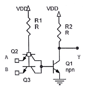
TTL (Transistor-Transistor Logic)
TTL was one of the earliest and most popular logic families, introduced in the 1960s. It uses bipolar junction transistors (BJTs) as the primary switching elements.
Key Characteristics:
| Parameter | Typical Value |
|---|---|
| Supply Voltage (VCC) | 5V ± 0.25V |
| Logic HIGH (VOH) | ≥ 2.4V |
| Logic LOW (VOL) | ≤ 0.4V |
| Input HIGH (VIH) | ≥ 2.0V |
| Input LOW (VIL) | ≤ 0.8V |
| Propagation Delay | 10-50 ns |
| Power Consumption | Moderate to High |
| Noise Margin | ~0.4V |
TTL Subfamilies:
- Standard TTL (74xx): Original family, moderate speed
- Low-Power TTL (74Lxx): Reduced power, slower speed
- High-Speed TTL (74Hxx): Faster but more power hungry
- Schottky TTL (74Sxx): Uses Schottky diodes for speed
- Low-Power Schottky (74LSxx): Best balance, very popular
- Advanced Low-Power Schottky (74ALSxx): Improved version
- Fast TTL (74Fxx): High speed for demanding applications
Each TTL subfamily represents a trade-off between speed, power consumption, and cost. The 74LSxx series became the most popular because it offered good speed with reasonable power consumption.
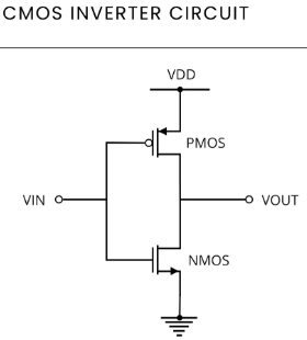
CMOS (Complementary Metal-Oxide-Semiconductor)
CMOS logic uses complementary pairs of MOSFETs (one N-channel, one P-channel) to implement logic functions. This is the dominant logic family today.
Key Characteristics:
| Parameter | Typical Value (5V CMOS) |
|---|---|
| Supply Voltage (VDD) | 3V to 18V (wide range) |
| Logic HIGH (VOH) | ≥ 4.95V (near VDD) |
| Logic LOW (VOL) | ≤ 0.05V (near GND) |
| Input HIGH (VIH) | ≥ 3.5V (70% VDD) |
| Input LOW (VIL) | ≤ 1.5V (30% VDD) |
| Propagation Delay | 25-100 ns (older), <1ns (modern) |
| Static Power | Nearly zero |
| Dynamic Power | Proportional to frequency |
| Noise Margin | ~30% of VDD |
CMOS Subfamilies:
- 4000 Series (CD4xxx): Original CMOS, slow but low power
- 74HC (High-Speed CMOS): CMOS replacement for TTL
- 74HCT: CMOS with TTL-compatible inputs
- 74AC (Advanced CMOS): Faster than HC
- 74ACT: AC with TTL-compatible inputs
- 74LVC (Low-Voltage CMOS): 3.3V and lower voltages
- 74AHC/AHCT: Advanced high-speed CMOS
CMOS became dominant because:
- Ultra-low static power consumption (only draws current when switching)
- Wide supply voltage range (3V to 18V for some families)
- Better noise margins (30% of supply vs. 0.4V for TTL)
- Scales well to smaller transistor sizes (modern CPUs are CMOS)
- Rail-to-rail output (outputs swing nearly full supply range)
Modern Low-Voltage Logic Families
As systems moved to lower voltages (3.3V, 2.5V, 1.8V) for power efficiency and semiconductor scaling, new families emerged:
| Family | Voltage | Common Use |
|---|---|---|
| 74LVC | 1.65-5.5V | General purpose, level translation |
| 74LVT | 2.7-3.6V | High-speed, TTL-compatible inputs |
| 74ALVC | 1.65-3.6V | Advanced low-voltage |
| 74AVC | 1.2-3.6V | Very high speed |
| 74AUP | 0.8-3.6V | Ultra-low power |
Critical Electrical Characteristics
1. Voltage Levels and Noise Margins
Understanding voltage levels is crucial for reliable digital design.
Voltage Level Definitions:
| Parameter | Description |
|---|---|
| VOH (min) | Minimum output voltage for HIGH |
| VOL (max) | Maximum output voltage for LOW |
| VIH (min) | Minimum input voltage recognized as HIGH |
| VIL (max) | Maximum input voltage recognized as LOW |
Noise Margin Calculation:
- High-level noise margin: NMH = VOH(min) - VIH(min)
- Low-level noise margin: NML = VIL(max) - VOL(max)
Larger noise margins mean your circuit is more immune to electrical noise. This is why CMOS (30% of VDD) is more robust than TTL (0.4V) in noisy environments.
2. Fan-Out and Loading
Fan-out is the number of gate inputs that can be driven by a single gate output without degrading performance.
For TTL:
- Determined by current: Each output must source/sink enough current for all inputs
- Typical fan-out: 10 for standard TTL, 20 for LS-TTL
For CMOS:
- Determined by capacitive loading and switching speed
- DC fan-out: Very high (>50) since inputs draw almost no DC current
- AC fan-out: Limited by rise/fall time degradation
Calculation Example:
If a 74LS00 NAND gate can sink 8mA (IOL) and each LS-TTL input requires 0.4mA (IIL):
In high-speed designs, even though CMOS has high DC fan-out, capacitive loading from multiple inputs can slow down your signals. Always check timing with realistic loads.
3. Propagation Delay
Propagation delay is the time it takes for an output to respond to an input change.
Two Key Measurements:
- tPLH: Propagation delay from LOW to HIGH output
- tPHL: Propagation delay from HIGH to LOW output
Typical Values:
| Logic Family | Propagation Delay |
|---|---|
| Standard TTL (74xx) | 10-15 ns |
| LS-TTL (74LSxx) | 9-10 ns |
| Fast TTL (74Fxx) | 3-5 ns |
| HC CMOS (74HCxx) | 8-12 ns |
| AC CMOS (74ACxx) | 3-5 ns |
| Modern FPGA logic | <1 ns |

4. Power Consumption
TTL Power Characteristics:
- Draws significant current in both states
- Power = VCC × ICC (relatively constant)
- Typical: 2-10mW per gate
CMOS Power Characteristics:
- Static power (not switching): Nearly zero (leakage only)
- Dynamic power (switching): P = C × V² × f
Where:
- C = load capacitance
- V = supply voltage
- f = switching frequency
A 74HC04 inverter at 5V driving 50pF at 1MHz:
At 10MHz: 12.5mW. Power scales linearly with frequency!
5. Switching Speed and Rise/Fall Times
Rise time (tr): Time for output to transition from 10% to 90% of final value
Fall time (tf): Time for output to transition from 90% to 10% of final value
Faster rise/fall times enable:
- Higher frequency operation
- Sharper clock edges
- But also more EMI and crosstalk
Comparison Table:
| Family | Rise/Fall Time | Max Frequency |
|---|---|---|
| Standard TTL | 5-10 ns | ~35 MHz |
| 74LSxx | 10-15 ns | ~25 MHz |
| 74HCxx | 5-8 ns | ~25 MHz |
| 74ACxx | 2-4 ns | ~100 MHz |
| Modern FPGA | <100 ps | >1 GHz |
Interfacing Different Logic Families
One of the most common real-world challenges is connecting circuits that use different logic families.
Case 1: TTL Driving CMOS
Problem: TTL VOH (2.4V typical) may not reach CMOS VIH (3.5V for 5V CMOS)
Solutions:
- Use 74HCT family (CMOS with TTL-compatible inputs)
- Add pull-up resistor to raise TTL output closer to 5V
- Use a level translator IC
Case 2: CMOS Driving TTL
Problem: CMOS cannot source enough current for TTL inputs
Solution:
- CMOS can typically drive 2-5 LS-TTL loads
- Use buffer if more drive needed
- Check datasheet for IOH (output high current)
Case 3: 5V to 3.3V Level Translation
Modern Reality: Many systems mix 5V legacy components with 3.3V microcontrollers
Solutions:
- Resistor divider (simple, one direction)
- 74LVCxx family (accepts 5V input with 3.3V supply)
- Bidirectional level shifters (TXS0108E, etc.)
- MOSFET-based shifters (for I2C, SPI)
Never directly connect 5V outputs to 3.3V CMOS inputs unless the datasheet explicitly states "5V tolerant inputs." You can damage the device!
Choosing the Right Logic Family
Decision Factors:
| Factor | Consider |
|---|---|
| Supply Voltage | Match your system voltage (5V, 3.3V, 1.8V) |
| Speed Requirements | Choose propagation delay accordingly |
| Power Budget | CMOS for battery, TTL less critical |
| Noise Environment | CMOS has better noise margins |
| Legacy Compatibility | Use HCT for TTL compatibility |
| Availability & Cost | Common families are cheaper |
| Temperature Range | Industrial or automotive grades available |
Common Application Choices:
| Application | Recommended Family |
|---|---|
| Hobby/Learning | 74HCxx (readily available) |
| 5V Microcontroller Interface | 74HCTxx |
| 3.3V Modern Systems | 74LVCxx, 74AHCxx |
| High-Speed (>50MHz) | 74ACxx, 74AVCxx |
| Battery-Powered | 74AUPxx (ultra-low power) |
| Mixed 5V/3.3V | 74LVCxx with level translation |
Practical Considerations
Input Protection
Never leave inputs floating! Unconnected inputs can:
- Float to intermediate voltages
- Oscillate due to noise pickup
- Cause excessive power consumption (especially CMOS)
- Lead to unpredictable behavior
Solutions:
- Tie unused inputs to VCC or GND through appropriate resistor
- Use pull-up/pull-down resistors for switch inputs
- Some families have built-in pull-ups (check datasheet)
Decoupling Capacitors
Always add decoupling capacitors:
- 0.1µF ceramic capacitor between VCC/VDD and GND
- Place close to each IC's power pin
- Add bulk capacitor (10-100µF) for every few ICs
ESD Protection
Digital ICs can be damaged by static discharge:
- Use ESD-safe handling procedures
- Some modern families include on-chip ESD protection
- Add external protection for exposed connectors
Summary
Logic families are the building blocks of digital systems. Understanding their characteristics helps you:
✅ Select appropriate components for your design
✅ Interface different voltage levels correctly
✅ Predict system performance (speed, power)
✅ Troubleshoot problems effectively
✅ Design reliable circuits that work in the real world
Key Takeaways:
- TTL: 5V only, moderate speed, higher power, good for legacy designs
- CMOS: Wide voltage range, ultra-low static power, excellent noise margins, industry standard
- Modern Logic: Low-voltage (3.3V, 1.8V), high-speed, power-efficient
- Interfacing: Always check voltage compatibility, use level shifters when needed
- Never: Leave inputs floating, exceed maximum ratings, ignore datasheet specifications
Now that you understand logic families, we're ready to dive into Boolean algebra and truth tables, which form the mathematical foundation for designing digital circuits.
Further Reading
- IC datasheets (Texas Instruments, NXP, ON Semiconductor)
- "Digital Integrated Circuits" by Jan Rabaey
- Application notes on level translation
- FPGA and CPLD family datasheets for modern high-speed logic
Practice Questions:
- Why does CMOS consume almost no static power?
- Calculate the noise margin for 5V CMOS given VOH=4.9V and VIH=3.5V
- Can you directly connect a 74LS00 output to a 74HC00 input? Why or why not?
- If a CMOS gate switches at 10MHz with 30pF load at 3.3V, what's the dynamic power?
- Why do we need 74HCT instead of 74HC when interfacing with TTL?